Q1 MHT CET 2026 · 13 MAY · SHIFT 1 Easy ☆
Junction Transistor · Structure & biasing
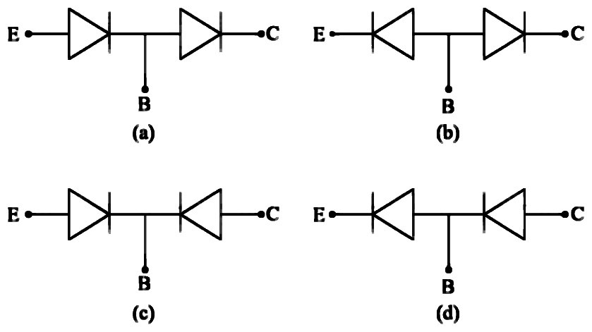
An n-p-n transistor can be considered to be equivalent to two diodes connected. Which one of the following figure is correct?
Show answer and solution
Answer: (b)
Loading the solution…
Report a mistake Q2 MHT CET 2026 · 19 APR · SHIFT 2 Easy ☆
Junction Transistor · Structure & biasing
In a transistor, comparing the doping of emitter, base and collector, the part which is heavily doped and that which is lightly doped are respectively
(a) collector and emitter (b) emitter and base (c) collector and base (d) emitter and collector Show answer and solution
Answer: (b)
Loading the solution…
Report a mistake Q3 MHT CET 2026 · 14 MAY · SHIFT 1 Easy ☆
Junction Transistor · Current relations
For a transistor, the current ratio α D C = 69 70 \alpha_{DC} = \frac{69}{70} α D C = 70 69 β D C \beta_{DC} β D C
(a) 66 66 66 (b) 67 67 67 (c) 69 69 69 (d) 71 71 71 Show answer and solution
Answer: (c)
Loading the solution…
Report a mistake Q4 MHT CET 2026 · 13 APR · SHIFT 2 Easy ☆
Junction Transistor · Current relations
If transistor having α = 0.9 \alpha = 0.9 α = 0.9 0.4 0.4 0.4
(a) 3.6 3.6 3.6 (b) 4 4 4 (c) 0.9 0.9 0.9 (d) 36 36 36 Show answer and solution
Answer: (a)
Loading the solution…
Report a mistake Q5 MHT CET 2026 · 13 APR · SHIFT 1 Easy ☆
Junction Transistor · Current relations
In transistor amplifier, base emitter junction is forward biased and collector base junction is reversed biased. The current gain is
(a) Δ I C Δ I B \frac{\Delta I_C}{\Delta I_B} Δ I B Δ I C (b) Δ I B Δ I C \frac{\Delta I_B}{\Delta I_C} Δ I C Δ I B (c) Δ I E Δ I B \frac{\Delta I_E}{\Delta I_B} Δ I B Δ I E (d) Δ I B Δ I E \frac{\Delta I_B}{\Delta I_E} Δ I E Δ I B Show answer and solution
Answer: (a)
Loading the solution…
Report a mistake Q6 MHT CET 2026 · 14 MAY · SHIFT 2 Easy ☆
Junction Transistor · CE amplifier gains
The current gain in the common emitter mode of a transistor is 10 10 10 20 k Ω 20\,k\Omega 20 k Ω 100 k Ω 100\,k\Omega 100 k Ω
(a) 300 300 300 (b) 500 500 500 (c) 200 200 200 (d) 100 100 100 Show answer and solution
Answer: (b)
Loading the solution…
Report a mistake Q7 MHT CET 2026 · 14 MAY · SHIFT 1 Easy ☆
Junction Transistor · CE amplifier gains
β , R L \beta, R_L β , R L r r r
(a) β ( R L / r ) \beta(R_L/r) β ( R L / r ) β 2 ( R L / r ) \beta^2(R_L/r) β 2 ( R L / r ) (b) β ( r / R L ) \beta(r/R_L) β ( r / R L ) β 2 ( r / R L ) \beta^2(r/R_L) β 2 ( r / R L ) (c) β ( R L / r ) \beta(R_L/r) β ( R L / r ) β ( R L / r ) 2 \beta(R_L/r)^2 β ( R L / r ) 2 (d) β ( r / R L ) \beta(r/R_L) β ( r / R L ) β ( r / R L ) 2 \beta(r/R_L)^2 β ( r / R L ) 2 Show answer and solution
Answer: (a)
Loading the solution…
Report a mistake Q8 MHT CET 2026 · 13 MAY · SHIFT 1 Easy ☆
Junction Transistor · CE amplifier gains
In common emitter amplifier, using output resistance 5000 Ω 5000\,\Omega 5000 Ω 2000 Ω 2000\,\Omega 2000 Ω 10 10 10 β = 50 \beta = 50 β = 50
(a) 5 × 1 0 − 6 5 \times 10^{-6} 5 × 1 0 − 6 (b) 12.50 × 1 0 − 6 12.50 \times 10^{-6} 12.50 × 1 0 − 6 (c) 1.25 1.25 1.25 (d) 125.0 125.0 125.0 Show answer and solution
Answer: (c)
Loading the solution…
Report a mistake Q9 MHT CET 2026 · 20 APR · SHIFT 1 Easy ☆
Junction Transistor · CE amplifier gains
In a common emitter transistor amplifier, AC current gain is 65 65 65 5400 Ω 5400\,\Omega 5400 Ω 450 Ω 450\,\Omega 450 Ω
(a) 460 460 460 (b) 540 540 540 (c) 780 780 780 (d) 7800 7800 7800 Show answer and solution
Answer: (c)
Loading the solution…
Report a mistake Q10 MHT CET 2026 · 17 APR · SHIFT 2 Easy ☆
Junction Transistor · CE amplifier gains
In common emitter configuration of transistor amplifier, r i , R L r_i, R_L r i , R L β \beta β A V A_V A V A P A_P A P
(a) β ( r i R L ) , β 2 ( r i R L ) \beta\left(\frac{r_i}{R_L}\right), \beta^2\left(\frac{r_i}{R_L}\right) β ( R L r i ) , β 2 ( R L r i ) (b) β ( R L r i ) , β ( R L r i ) 2 \beta\left(\frac{R_L}{r_i}\right), \beta\left(\frac{R_L}{r_i}\right)^2 β ( r i R L ) , β ( r i R L ) 2 (c) β ( R L r i ) , β 2 ( R L r i ) \beta\left(\frac{R_L}{r_i}\right), \beta^2\left(\frac{R_L}{r_i}\right) β ( r i R L ) , β 2 ( r i R L ) (d) β ( r i R L ) , β ( r i R L ) 2 \beta\left(\frac{r_i}{R_L}\right), \beta\left(\frac{r_i}{R_L}\right)^{2} β ( R L r i ) , β ( R L r i ) 2 Show answer and solution
Answer: (c)
Loading the solution…
Report a mistake Q11 MHT CET 2026 · 13 MAY · SHIFT 2 Medium ☆
Junction Transistor · Current relations
In an n-p-n transistor the collector current is 9 9 9 90 % 90\% 90%
(a) β = 9.0 \beta = 9.0 β = 9.0 (b) the base current is 10 10 10 (c) the emitter current is 1 1 1 (d) β = 0.9 \beta = 0.9 β = 0.9 Show answer and solution
Answer: (a)
Loading the solution…
Report a mistake Q12 MHT CET 2026 · 18 APR · SHIFT 2 Medium ☆
Junction Transistor · Current relations
In an NPN transistor, the collector current is 28 mA. If 80% electrons reach the collector, its base current in mA is
(a) 7 7 7 (b) 14 14 14 (c) 28 28 28 (d) 35 35 35 Show answer and solution
Answer: (a)
Loading the solution…
Report a mistake Q13 MHT CET 2026 · 13 APR · SHIFT 1 Medium ☆
Junction Transistor · Current relations
In common emitter mode of transistor, the d.c. current gain is 20, the emitter current is 7 mA. The collector current is
(a) 20 3 \frac{20}{3} 3 20 (b) 14 5 \frac{14}{5} 5 14 (c) 1 3 \frac{1}{3} 3 1 (d) 8 13 \frac{8}{13} 13 8 Show answer and solution
Answer: (a)
Loading the solution…
Report a mistake Q14 MHT CET 2026 · 11 APR · SHIFT 2 Medium ☆
Junction Transistor · Current relations
In common emitter mode of transistor, the d.c. current gain is 20 20 20 7 7 7
(a) 14 3 \frac{14}{3} 3 14 (b) 20 3 \frac{20}{3} 3 20 (c) 7 3 \frac{7}{3} 3 7 (d) 8 3 \frac{8}{3} 3 8 Show answer and solution
Answer: (b)
Loading the solution…
Report a mistake Q15 MHT CET 2026 · 16 APR · SHIFT 1 Medium ☆
Junction Transistor · CE amplifier gains
In a transistor amplifier, a change of 0.2 mA in the base current causes a change of 5 mA in the collector current. If input resistance is 2 2 2 Ω \Omega Ω
(a) 4 4 4 Ω \Omega Ω (b) 6 6 6 Ω \Omega Ω (c) 8 8 8 Ω \Omega Ω (d) 2 2 2 Ω \Omega Ω Show answer and solution
Answer: (b)
Loading the solution…
Report a mistake Q16 MHT CET 2026 · 15 APR · SHIFT 2 Medium ☆
Junction Transistor · CE amplifier gains
In common emitter amplifier, a change of 0.2 0.2 0.2 5 5 5 2 2 2 Ω \Omega Ω 75 75 75
(a) 2 2 2 Ω \Omega Ω (b) 3 3 3 Ω \Omega Ω (c) 4 4 4 Ω \Omega Ω (d) 6 6 6 Ω \Omega Ω Show answer and solution
Answer: (d)
Loading the solution…
Report a mistake Q17 MHT CET 2026 · 11 APR · SHIFT 1 Medium ☆
Junction Transistor · CE amplifier gains
In common emitter transistor amplifier, the output resistance is 500 500 500 Ω \Omega Ω β = 50 \beta = 50 β = 50 5 × 1 0 6 5 \times 10^{6} 5 × 1 0 6
(a) 325 Ω 325\ \Omega 325 Ω (b) 150 Ω 150\ \Omega 150 Ω (c) 350 Ω 350\ \Omega 350 Ω (d) 250 Ω 250\ \Omega 250 Ω Show answer and solution
Answer: (d)
Loading the solution…
Report a mistake Q18 MHT CET 2026 · 15 MAY · SHIFT 1 Medium ☆
Junction Transistor · Characteristics & transistor testing
In an n-p-n transistor in common emitter configuration when V B E V_{BE} V BE
(a) I B I_B I B I C I_C I C (b) I B I_B I B I C I_C I C (c) I B I_B I B I C I_C I C (d) both I B I_B I B I C I_C I C Show answer and solution
Answer: (a)
Loading the solution…
Report a mistake Q19 MHT CET 2025 · 26 APR · SHIFT 2 Easy ☆
Junction Transistor · Current relations
For a transistor, α dc \alpha_\text{dc} α dc β dc \beta_\text{dc} β dc β dc − α dc α dc × β dc \frac{\beta_\text{dc} - \alpha_\text{dc}}{\alpha_\text{dc} \times \beta_\text{dc}} α dc × β dc β dc − α dc
Show answer and solution
Answer: (d)
Loading the solution…
Report a mistake Q20 MHT CET 2025 · 23 APR · SHIFT 1 Easy ☆
Junction Transistor · Current relations
In a common emitter transistor amplifier circuit, the current gain α = 0.8 \alpha = 0.8 α = 0.8 3 μ A 3\,\mu\text{A} 3 μ A
(a) 4 μ A 4\,\mu\text{A} 4 μ A (b) 12 μ A 12\,\mu\text{A} 12 μ A (c) 6 μ A 6\,\mu\text{A} 6 μ A (d) 24 μ A 24\,\mu\text{A} 24 μ A Show answer and solution
Answer: (b)
Loading the solution…
Report a mistake Q21 MHT CET 2025 · 23 APR · SHIFT 1 Easy ☆
Junction Transistor · Current relations
In the case of common emitter transistor amplifier, the ratio of collector current to emitter current is 0.96, then the current gain ( β ) (\beta) ( β )
Show answer and solution
Answer: (c)
Loading the solution…
Report a mistake Q22 MHT CET 2025 · 19 APR · SHIFT 1 Easy ☆
Junction Transistor · Current relations
For a common emitter transistor, if I C I E = 0.95 \frac{I_\text{C}}{I_\text{E}} = 0.95 I E I C = 0.95
Show answer and solution
Answer: (c)
Loading the solution…
Report a mistake Q23 MHT CET 2025 · 19 APR · SHIFT 1 Easy ☆
Junction Transistor · Current relations
In the case of constant ' α \alpha α β \beta β α \alpha α β \beta β
(a) β < 1 , α > 1 \beta < 1, \alpha > 1 β < 1 , α > 1 (b) β > 1 , α < 1 \beta > 1, \alpha < 1 β > 1 , α < 1 (c) α = β \alpha = \beta α = β (d) α = β 2 \alpha = \beta^2 α = β 2 Show answer and solution
Answer: (b)
Loading the solution…
Report a mistake Q24 MHT CET 2025 · 22 APR · SHIFT 1 Easy ☆
Junction Transistor · CE amplifier gains
In a common emitter transistor amplifier, the output voltage and input voltage have a phase difference of
(a) 0 c 0^{c} 0 c (b) π c 2 \frac{\pi^{c}}{2} 2 π c (c) 3 π c 4 \frac{3\pi^{c}}{4} 4 3 π c (d) π c \pi^{c} π c Show answer and solution
Answer: (d)
Loading the solution…
Report a mistake Q25 MHT CET 2025 · 21 APR · SHIFT 2 Easy ☆
Junction Transistor · CE amplifier gains
In common emitter mode of a transistor, the current gain is 8. The input impedance is 25 k Ω 25\text{ k}\Omega 25 k Ω 75 k Ω 75\text{ k}\Omega 75 k Ω
Show answer and solution
Answer: (a)
Loading the solution…
Report a mistake Q26 MHT CET 2025 · 20 APR · SHIFT 1 Easy ☆
Junction Transistor · CE amplifier gains
When an n-p-n junction transistor is used as an amplifier in common emitter mode,
(a) the base emitter junction is reverse biased. (b) the input impedance is high and the output impedance is low. (c) input signal is applied between the base and emitter and the output is obtained between collector and emitter. (d) the input voltage and the output voltage are in phase. Show answer and solution
Answer: (c)
Loading the solution…
Report a mistake Q27 MHT CET 2025 · 19 APR · SHIFT 2 Easy ☆
Junction Transistor · CE amplifier gains
In a transistor amplifier, AC current gain is 64, the load resistance is 5400 Ω 5400\ \Omega 5400 Ω 540 Ω 540\ \Omega 540 Ω
(a) 540 (b) 600 (c) 640 (d) 6400 Show answer and solution
Answer: (c)
Loading the solution…
Report a mistake Q28 MHT CET 2025 · 21 APR · SHIFT 1 Medium ☆
Junction Transistor · Current relations
In an n-p-n transistor amplifier, the collector current is 8 mA. If 80 % 80\% 80% α \alpha α β \beta β
(a) the base current is 20 mA. (b) the emitter current is 2 mA. (c) α = 0.8 , β = 4.0 \alpha = 0.8, \beta = 4.0 α = 0.8 , β = 4.0 (d) α = 4.0 , β = 0.8 \alpha = 4.0, \beta = 0.8 α = 4.0 , β = 0.8 Show answer and solution
Answer: (c)
Loading the solution…
Report a mistake Q29 MHT CET 2025 · 20 APR · SHIFT 2 Medium ☆
Junction Transistor · Current relations
In an n-p-n transistor amplifier, the collector current is 9 mA. If 90 % 90\% 90%
(a) α = 9 , β = 0.9 \alpha = 9, \beta = 0.9 α = 9 , β = 0.9 (b) α = 0.9 , β = 90 \alpha = 0.9, \beta = 90 α = 0.9 , β = 90 (c) α = 0.9 , β = 9 \alpha = 0.9, \beta = 9 α = 0.9 , β = 9 (d) α = 90 , β = 0.9 \alpha = 90, \beta = 0.9 α = 90 , β = 0.9 Show answer and solution
Answer: (c)
Loading the solution…
Report a mistake Q30 MHT CET 2025 · 26 APR · SHIFT 1 Medium ☆
Junction Transistor · CE amplifier gains
In a common emitter transistor amplifier circuit, the input resistance is 1.8 k Ω 1.8\text{ k}\Omega 1.8 k Ω 9 k Ω 9\text{ k}\Omega 9 k Ω
(a) 0.7 V (b) 1.4 V (c) 2.1 V (d) 4.2 V Show answer and solution
Answer: (c)
Loading the solution…
Report a mistake Q31 MHT CET 2025 · 25 APR · SHIFT 2 Medium ☆
Junction Transistor · CE amplifier gains
In a common emitter amplifier configuration, the current gain is 62. The collector resistance and input resistance are 5 k Ω 5\text{ k}\Omega 5 k Ω 500 Ω 500\ \Omega 500 Ω
(a) 0.62 V (b) 6.2 V (c) 62 V (d) 620 V Show answer and solution
Answer: (b)
Loading the solution…
Report a mistake Q32 MHT CET 2025 · 20 APR · SHIFT 1 Medium ☆
Junction Transistor · CE amplifier gains
In a transistor (common emitter configuration) the ratio of power gain to voltage gain is ( α \alpha α β \beta β
(a) β α \frac{\beta}{\alpha} α β (b) α β \alpha\beta α β (c) α \alpha α (d) β \beta β Show answer and solution
Answer: (d)
Loading the solution…
Report a mistake Q33 MHT CET 2024 · 3 MAY · SHIFT 1 Easy ☆
Junction Transistor · Structure & biasing
An n-p-n transistor can be considered to be equivalent to two diodes connected. The correct figure out of the following is
Show answer and solution
Answer: (b)
Loading the solution…
Report a mistake Q34 MHT CET 2024 · 15 MAY · SHIFT 1 Easy ☆
Junction Transistor · Current relations
For a transistor, current gain ( β ) = 50 (\beta) = 50 ( β ) = 50 350 μ A 350\,\mu\text{A} 350 μ A
(a) ( 50 350 ) μ A \left(\frac{50}{350}\right)\mu\text{A} ( 350 50 ) μ A (b) ( 350 − 50 ) μ A (350 - 50)\,\mu\text{A} ( 350 − 50 ) μ A (c) ( 350 + 50 ) μ A (350 + 50)\,\mu\text{A} ( 350 + 50 ) μ A (d) ( 350 50 ) μ A \left(\frac{350}{50}\right)\mu\text{A} ( 50 350 ) μ A Show answer and solution
Answer: (d)
Loading the solution…
Report a mistake Q35 MHT CET 2024 · 16 MAY · SHIFT 1 Easy ☆
Junction Transistor · CE amplifier gains
The input signal given to C.E. amplifier having a voltage gain of 126 is V i = 2 cos ( 12 t + π 3 ) V_i = 2\cos\left(12t + \frac{\pi}{3}\right) V i = 2 cos ( 12 t + 3 π )
(a) 252 cos ( 12 t + 4 π 3 ) 252\cos\left(12t + \frac{4\pi}{3}\right) 252 cos ( 12 t + 3 4 π ) (b) 252 cos ( 12 t + π 3 ) 252\cos\left(12t + \frac{\pi}{3}\right) 252 cos ( 12 t + 3 π ) (c) 63 cos ( 12 t + 2 π 3 ) 63\cos\left(12t + \frac{2\pi}{3}\right) 63 cos ( 12 t + 3 2 π ) (d) 2 cos ( 12 t + 5 π 3 ) 2\cos\left(12t + \frac{5\pi}{3}\right) 2 cos ( 12 t + 3 5 π ) Show answer and solution
Answer: (a)
Loading the solution…
Report a mistake Q36 MHT CET 2024 · 11 MAY · SHIFT 2 Easy ☆
Junction Transistor · CE amplifier gains
When n-p-n junction transistor is used as an amplifier in common emitter mode,
(a) the input impedance is high and the output impedance is low. (b) the base emitter junction is reverse biased. (c) input signal is applied between the base and emitter and output is obtained between collector and emitter. (d) the input voltage and output voltage are in phase. Show answer and solution
Answer: (c)
Loading the solution…
Report a mistake Q37 MHT CET 2024 · 3 MAY · SHIFT 1 Easy ☆
Junction Transistor · CE amplifier gains
In common emitter transistor amplifier, load resistance is 6.5 k Ω 6.5\text{ k}\Omega 6.5 k Ω 1.3 k Ω 1.3\text{ k}\Omega 1.3 k Ω
Show answer and solution
Answer: (b)
Loading the solution…
Report a mistake Q38 MHT CET 2024 · 4 MAY · SHIFT 1 Medium ☆
Junction Transistor · Current relations
The collector supply voltage is 6 V and a voltage drop across a resistor of 600 Ω 600\ \Omega 600 Ω
(a) 0.25 mA (b) 0.05 mA (c) 0.12 mA (d) 0.02 mA Show answer and solution
Answer: (b)
Loading the solution…
Report a mistake Q39 MHT CET 2024 · 2 MAY · SHIFT 1 Medium ☆
Junction Transistor · Current relations
In an NPN transistor 1 0 10 10^{10} 1 0 10 1 0 − 6 s 10^{-6}\text{ s} 1 0 − 6 s 2 % 2\% 2% α \alpha α β \beta β
(a) 0.98 , 49 0.98, 49 0.98 , 49 (b) 49 , 0.98 49, 0.98 49 , 0.98 (c) 0.49 , 98 0.49, 98 0.49 , 98 (d) 98 , 0.49 98, 0.49 98 , 0.49 Show answer and solution
Answer: (a)
Loading the solution…
Report a mistake Q40 MHT CET 2024 · 9 MAY · SHIFT 1 Medium ☆
Junction Transistor · CE amplifier gains
The current amplification factor of a transistor is 50. The input resistance when used in common emitter mode is 1 k Ω 1\text{ k}\Omega 1 k Ω
(a) 100 μ A 100\ \mu\text{A} 100 μ A (b) 0.01 mA (c) 0.25 mA (d) 500 μ A 500\ \mu\text{A} 500 μ A Show answer and solution
Answer: (d)
Loading the solution…
Report a mistake Q41 JEE Main 2023 · 31 JAN · SHIFT 2 Easy Old syllabus ☆
Junction Transistor · Structure & biasing
Given below are two statements:
Statement I: In a typical transistor, all three regions emitter, base and collector have same doping level.
Statement II: In a transistor, collector is the thickest and base is the thinnest segment. In the light of the above statements, choose the most appropriate answer from the options given below.
(a) Statement I is correct but Statement II is incorrect (b) Both Statement I and Statement II are incorrect (c) Statement I is incorrect but Statement II is correct (d) Both Statement I and Statement II are correct Show answer and solution
Answer: (c)
Loading the solution…
Report a mistake Q42 MHT CET 2023 · 14 MAY · SHIFT 1 Easy ☆
Junction Transistor · Current relations
For a common emitter configuration, if 'α \alpha α β \beta β α \alpha α β \beta β
(a) 1 α = 1 β + 1 \frac{1}{\alpha} = \frac{1}{\beta} + 1 α 1 = β 1 + 1 (b) α = β 1 − β \alpha = \frac{\beta}{1-\beta} α = 1 − β β (c) α = β 1 + β \alpha = \frac{\beta}{1+\beta} α = 1 + β β (d) 1 β = 1 α − 1 \frac{1}{\beta} = \frac{1}{\alpha} - 1 β 1 = α 1 − 1 Show answer and solution
Answer: (b)
Loading the solution…
Report a mistake Q43 MHT CET 2023 · 11 MAY · SHIFT 2 Easy ☆
Junction Transistor · Current relations
In the study of transistor as an amplifier if α = I C I E = 0.98 \alpha = \frac{I_C}{I_E} = 0.98 α = I E I C = 0.98 β = I C I B = 49 \beta = \frac{I_C}{I_B} = 49 β = I B I C = 49 I C , I B I_C, I_B I C , I B I E \text{I}_\text{E} I E ( 1 α − 1 β ) \left(\frac{1}{\alpha} - \frac{1}{\beta}\right) ( α 1 − β 1 )
(a) zero (b) 1 2 \frac{1}{2} 2 1 (c) 2 (d) 1 Show answer and solution
Answer: (d)
Loading the solution…
Report a mistake Q44 JEE Main 2023 · 12 APR · SHIFT 1 Easy Old syllabus ☆
Junction Transistor · Current relations
In an n-p-n common emitter (CE) transistor the collector current changes from 5 mA \text{mA} mA 16 mA 16\text{ mA} 16 mA 100 μ A 100\,\mu\text{A} 100 μ A 200 μ A 200\,\mu\text{A} 200 μ A
Show answer and solution
Answer: (d)
Loading the solution…
Report a mistake Q45 MHT CET 2023 · 9 MAY · SHIFT 2 Easy ☆
Junction Transistor · CE amplifier gains
In a transistor, in common emitter configuration, the ratio of power gain to voltage gain is
(a) α \alpha α (b) β α \frac{\beta}{\alpha} α β (c) β α \beta\alpha β α (d) β \beta β Show answer and solution
Answer: (d)
Loading the solution…
Report a mistake Q46 MHT CET 2023 · 10 MAY · SHIFT 2 Medium ☆
Junction Transistor · Structure & biasing
Which one of the operations of n − p − n \mathrm{n}-\mathrm{p}-\mathrm{n} n − p − n p − n − p p-n-p p − n − p
(a) The emitter-base junction is reversed biased in n − p − n \mathrm{n}-\mathrm{p}-\mathrm{n} n − p − n (b) The emitter injects minority carriers into the base region of the p − n − p \mathrm{p}-\mathrm{n}-\mathrm{p} p − n − p (c) The emitter injects holes into the base of the p − n − p \mathrm{p}-\mathrm{n}-\mathrm{p} p − n − p n − p − n n-p-n n − p − n (d) The emitter injects holes into the base of n − p − n \mathrm{n}-\mathrm{p}-\mathrm{n} n − p − n Show answer and solution
Answer: (c)
Loading the solution…
Report a mistake Q47 NEET 2023 Medium Old syllabus ☆
Junction Transistor · Structure & biasing
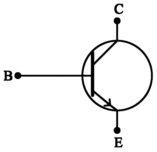
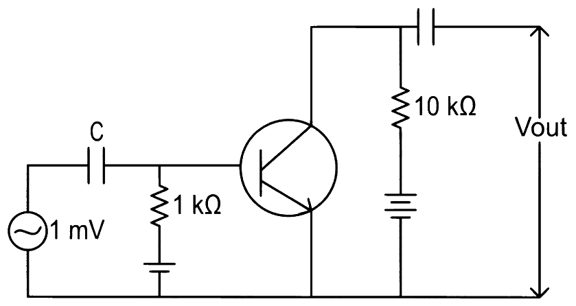
The above figure shows the circuit symbol of a transistor. Select the correct statements given below:
(A) The transistor has two segments of p-type semiconductor separated by a segment of n-type semiconductor.
(B) The emitter is of moderate size and heavily doped.
(C) The central segment is thin and lightly doped.
(D) The emitter base junction is reverse biased in common emitter amplifier circuit.
(a) (C) and (D) (b) (A) and (D) (c) (A) and (B) (d) (B) and (C) Show answer and solution
Answer: (d)
Loading the solution…
Report a mistake Q48 MHT CET 2023 · 14 MAY · SHIFT 2 Medium ☆
Junction Transistor · Current relations
In an n-p-n transistor, the collector current is 28 mA 28\text{ mA} 28 mA 80 % 80\% 80% mA \text{mA} mA
Show answer and solution
Answer: (d)
Loading the solution…
Report a mistake Q49 JEE Main 2023 · 8 APR · SHIFT 2 Medium Old syllabus ☆
Junction Transistor · CE amplifier gains
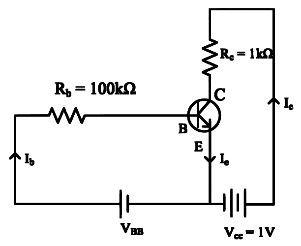
For a given transistor amplifier circuit in CE \text{CE} CE V C C = 1 V , R C = 1 k Ω , R b = 100 k Ω \mathrm{V}_{\mathrm{CC}} = 1\text{ V}, \mathrm{R}_{\mathrm{C}} = 1\text{ k}\Omega, \mathrm{R}_{\mathrm{b}} = 100\text{ k}\Omega V CC = 1 V , R C = 1 k Ω , R b = 100 k Ω β = 100 \beta = 100 β = 100 I b \mathrm{I}_{\mathrm{b}} I b
(a) I b = 100 μ A \mathrm{I}_{\mathrm{b}} = 100\ \mu\text{A} I b = 100 μ A (b) I b = 0.1 μ A \mathrm{I}_{\mathrm{b}} = 0.1\ \mu\text{A} I b = 0.1 μ A (c) I b = 1.0 μ A \mathrm{I}_{\mathrm{b}} = 1.0\ \mu\text{A} I b = 1.0 μ A (d) I b = 10 μ A \mathrm{I}_{\mathrm{b}} = 10\ \mu\text{A} I b = 10 μ A Show answer and solution
Answer: (d)
Loading the solution…
Report a mistake Q50 JEE Main 2023 · 13 APR · SHIFT 1 Medium Old syllabus ☆
Junction Transistor · Characteristics & transistor testing
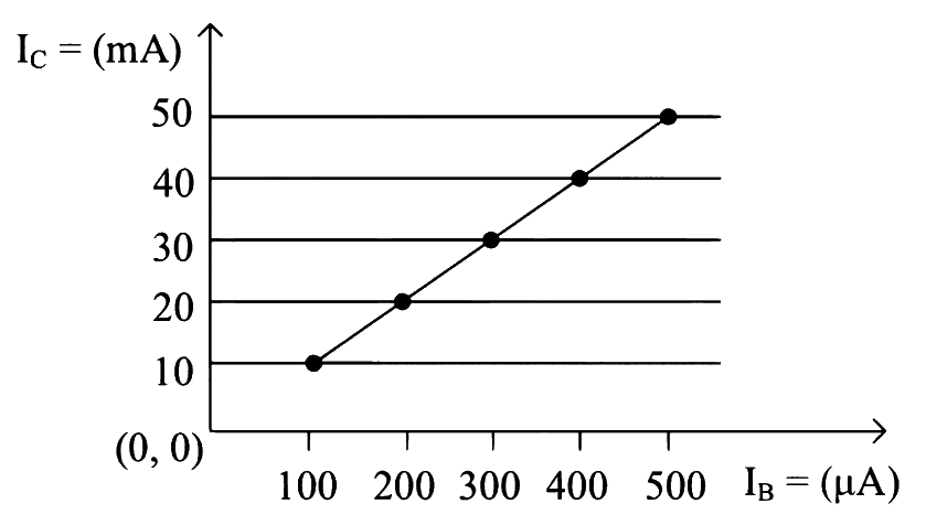
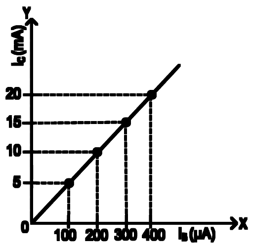
From the given transfer characteristic of a transistor in CE \text{CE} CE 1 0 x 10^{x} 1 0 x R B = 10 k Ω \mathrm{R}_{\mathrm{B}} = 10\text{ k}\Omega R B = 10 k Ω R C = 1 k Ω \mathrm{R}_{\mathrm{C}} = 1\text{ k}\Omega R C = 1 k Ω x x x
Numerical answer type. Work it out, then open the answer.
Show answer and solution
Answer: 3
Loading the solution…
Report a mistake Q51 JEE Main 2022 · 27 JUL · SHIFT 2 Easy Old syllabus ☆
Junction Transistor · Current relations
For a constant collector-emitter voltage of 8 V 8\text{ V} 8 V 6 mA 6\text{ mA} 6 mA 4 mA 4\text{ mA} 4 mA 20 μ A 20\,\mu\text{A} 20 μ A 25 μ A 25\,\mu\text{A} 25 μ A
(a) 240 (b) 400 (c) 0.0025 (d) 200 Show answer and solution
Answer: (b)
Loading the solution…
Report a mistake Q52 JEE Main 2022 · 27 JUN · SHIFT 2 Easy Old syllabus ☆
Junction Transistor · Switch & oscillator
For a transistor to act as a switch, it must be operated in
(a) Active region. (b) Saturation state only. (c) Cut-off state only. (d) Saturation and cut-off state. Show answer and solution
Answer: (d)
Loading the solution…
Report a mistake Q53 JEE Main 2022 · 26 JUN · SHIFT 2 Easy Old syllabus ☆
Junction Transistor · Switch & oscillator
The positive feedback is required by an amplifier to act an oscillator. The feedback here means:
(a) External input is necessary to sustain ac signal in output. (b) A portion of the output power is returned back to the input. (c) Feedback can be achieved by LR network. (d) The base-collector junction must be forward biased. Show answer and solution
Answer: (b)
Loading the solution…
Report a mistake Q54 JEE Main 2022 · 28 JUN · SHIFT 1 Medium Old syllabus ☆
Junction Transistor · Structure & biasing
Given below are two statements: One is labelled as Assertion A and the other is labelled as Reason R.
Assertion A: n-p-n transistor permits more current than a p-n-p transistor.
Reason R: Electrons have greater mobility as a charge carrier.
Choose the correct answer from the options given below:
(a) Both A and R are true, and R is correct explanation of A. (b) Both A and R are true but R is NOT the correct explanation of A. (c) A is true but R is false. (d) A is false but R is true. Show answer and solution
Answer: (a)
Loading the solution…
Report a mistake Q55 NEET 2022 · PHASE 2 Medium Old syllabus ☆
Junction Transistor · CE amplifier gains
The collector current in a common base amplifier using n-p-n transistor is 24 mA. If 80% of the electrons released by the emitter is accepted by the collector, then the base current is numerically:
(a) 3 mA and entering the base (b) 6 mA and leaving the base (c) 3 mA and leaving the base (d) 6 mA and entering the base Show answer and solution
Answer: (d)
Loading the solution…
Report a mistake Q56 JEE Main 2022 · 28 JUL · SHIFT 2 Medium Old syllabus ☆
Junction Transistor · CE amplifier gains
An n.p.n transistor with current gain β = 100 \beta = 100 β = 100
(a) 0.1 V (b) 1.0 V (c) 10 V (d) 100 V Show answer and solution
Answer: (b)
Loading the solution…
Report a mistake Q57 JEE Main 2022 · 29 JUN · SHIFT 1 Medium Old syllabus ☆
Junction Transistor · CE amplifier gains
A transistor is used in an amplifier circuit in common emitter mode. If the base current changes by 100 μ \mu μ Ω \Omega Ω Ω \Omega Ω × \times ×
Numerical answer type. Work it out, then open the answer.
Show answer and solution
Answer: 2
Loading the solution…
Report a mistake Q58 JEE Main 2022 · 24 JUN · SHIFT 1 Medium Old syllabus ☆
Junction Transistor · CE amplifier gains
A transistor is used in common-emitter mode in an amplifier circuit. When a signal of 10 mV is added to the base-emitter voltage, the base current changes by 10 μ \mu μ Ω \Omega Ω
Numerical answer type. Work it out, then open the answer.
Show answer and solution
Answer: 750
Loading the solution…
Report a mistake Q59 JEE Main 2022 · 26 JUL · SHIFT 2 Medium Old syllabus ☆
Junction Transistor · Characteristics & transistor testing
The typical transfer characteristics of a transistor in CE configuration is shown in figure. A load resistor of 2 k Ω 2\text{ k}\Omega 2 k Ω 0.50 k Ω 0.50\text{ k}\Omega 0.50 k Ω
Numerical answer type. Work it out, then open the answer.
Show answer and solution
Answer: 200
Loading the solution…
Report a mistake Q60 JEE Main 2022 · 25 JUN · SHIFT 2 Medium Old syllabus ☆
Junction Transistor · Characteristics & transistor testing
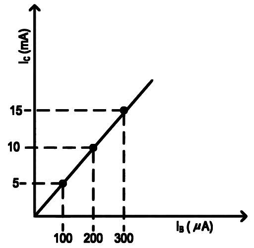
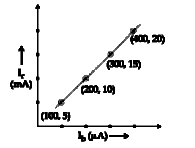
In an experiment of CE configuration of n-p-n transistor, the transfer characteristics are observed as given in figure.
If the input resistance is 200 Ω \Omega Ω Ω \Omega Ω
Numerical answer type. Work it out, then open the answer.
Show answer and solution
Answer: 15
Loading the solution…
Report a mistake Q61 MHT CET 2021 · 24 SEP · SHIFT 2 Easy ☆
Junction Transistor · Current relations
For a transistor, the current ratio α dc = 69 70 \alpha_\text{dc} = \frac{69}{70} α dc = 70 69 β dc \beta_\text{dc} β dc
Show answer and solution
Answer: (b)
Loading the solution…
Report a mistake Q62 MHT CET 2021 · 21 SEP · SHIFT 1 Easy ☆
Junction Transistor · Current relations
For a transistor, 1 α DC − 1 β DC \frac{1}{\alpha_\text{DC}} - \frac{1}{\beta_\text{DC}} α DC 1 − β DC 1 α DC \alpha_\text{DC} α DC β DC \beta_\text{DC} β DC
(a) three (b) two (c) zero (d) one Show answer and solution
Answer: (d)
Loading the solution…
Report a mistake Q63 JEE Main 2021 · 27 AUG · SHIFT 2 Easy Old syllabus ☆
Junction Transistor · Current relations
For a transistor α \alpha α β \beta β α = I C I E \alpha = \frac{I_C}{I_E} α = I E I C β = I C I B \beta = \frac{I_C}{I_B} β = I B I C α \alpha α β \beta β
(a) α = 1 − β β \alpha = \frac{1-\beta}{\beta} α = β 1 − β (b) β = α 1 − α \beta = \frac{\alpha}{1-\alpha} β = 1 − α α (c) α β = 1 \alpha\beta = 1 α β = 1 (d) α = β 1 − β \alpha = \frac{\beta}{1-\beta} α = 1 − β β Show answer and solution
Answer: (b)
Loading the solution…
Report a mistake Q64 JEE Main 2021 · 18 MAR · SHIFT 2 Easy Old syllabus ☆
Junction Transistor · Current relations
The correct relation between α \alpha α β \beta β
(a) β = α 1 + α \beta = \frac{\alpha}{1+\alpha} β = 1 + α α (b) α = β 1 − α \alpha = \frac{\beta}{1-\alpha} α = 1 − α β (c) α = β 1 + β \alpha = \frac{\beta}{1+\beta} α = 1 + β β (d) β = 1 1 − α \beta = \frac{1}{1-\alpha} β = 1 − α 1 Show answer and solution
Answer: (c)
Loading the solution…
Report a mistake Q65 JEE Main 2021 · 24 FEB · SHIFT 1 Easy Old syllabus ☆
Junction Transistor · Current relations
If an emitter current is changed by 4 mA, the collector current changes by 3.5 mA. The value of β \beta β
Show answer and solution
Answer: (d)
Loading the solution…
Report a mistake Q66 MHT CET 2021 · 22 SEP · SHIFT 2 Easy ☆
Junction Transistor · CE amplifier gains
For a common-emitter amplifier, the voltage gain is 40. Its input and output impedances are 100 Ω 100\ \Omega 100 Ω 400 Ω 400\ \Omega 400 Ω
Show answer and solution
Answer: (b)
Loading the solution…
Report a mistake Q67 JEE Main 2021 · 27 AUG · SHIFT 1 Easy Old syllabus ☆
Junction Transistor · CE amplifier gains
For a transistor in CE mode to be used as an amplifier, it must be operated in:
(a) Both cut-off and Saturation (b) Saturation region only (c) Cut-off region only (d) The active region only Show answer and solution
Answer: (d)
Loading the solution…
Report a mistake Q68 JEE Main 2021 · 24 FEB · SHIFT 2 Medium Old syllabus ☆
Junction Transistor · Structure & biasing
Given below are two statements:
Statement I: PN junction diodes can be used to function as transistor, simply by connecting two diodes, back to back, which acts as the base terminal.
Statement II: In the study of transistor, the amplification factor β \beta β
In the light of the above statements, choose the correct answer from the options given below.
(a) Both Statement I and Statement II are false (b) Statement I is false but Statement II is true (c) Both Statement I and Statement II are true (d) Statement I is true but Statement II is false Show answer and solution
Answer: (b)
Loading the solution…
Report a mistake Q69 MHT CET 2021 · 23 SEP · SHIFT 2 Medium ☆
Junction Transistor · Current relations
In a CE transistor, a change of 8.0 mA 8.0\text{ mA} 8.0 mA 7.8 mA 7.8\text{ mA} 7.8 mA
(a) 200 μ A 200\ \mu\text{A} 200 μ A (b) 50 μ A 50\ \mu\text{A} 50 μ A (c) 100 μ A 100\ \mu\text{A} 100 μ A (d) 150 μ A 150\ \mu\text{A} 150 μ A Show answer and solution
Answer: (a)
Loading the solution…
Report a mistake Q70 JEE Main 2021 · 27 JUL · SHIFT 1 Medium Old syllabus ☆
Junction Transistor · Current relations
A transistor is connected in common emitter circuit configuration, the collector supply voltage is 10 V and the voltage drop across a resistor of 1000 Ω \Omega Ω β \beta β μ \mu μ
Numerical answer type. Work it out, then open the answer.
Show answer and solution
Answer: 25
Loading the solution…
Report a mistake Q71 MHT CET 2021 · 23 SEP · SHIFT 1 Medium ☆
Junction Transistor · CE amplifier gains
In common emitter amplifier, a change of 0.2 mA in the base current causes a change of 5 mA in the collector current. If input resistance is 2 kΩ \Omega Ω
(a) 8 kΩ \Omega Ω (b) 4 kΩ \Omega Ω (c) 12 kΩ \Omega Ω (d) 6 kΩ \Omega Ω Show answer and solution
Answer: (d)
Loading the solution…
Report a mistake Q72 JEE Main 2021 · 18 MAR · SHIFT 1 Medium Old syllabus ☆
Junction Transistor · CE amplifier gains
An npn transistor operates as a common emitter amplifier with a power gain of 106. The input circuit resistance is 100Ω \Omega Ω Ω \Omega Ω β \beta β
Numerical answer type. Work it out, then open the answer.
Show answer and solution
Answer: 100
Loading the solution…
Report a mistake Q73 JEE Main 2021 · 18 MAR · SHIFT 2 Medium Old syllabus ☆
Junction Transistor · Characteristics & transistor testing
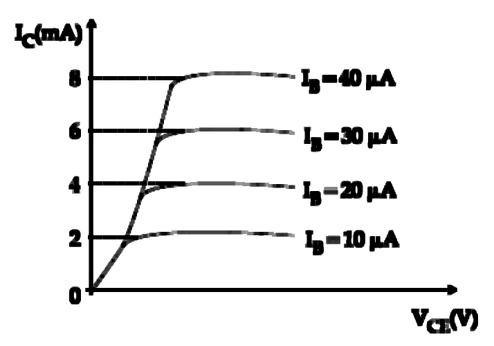
The typical output characteristics curve for a transistor working in the common-emitter configuration is shown in the figure.
The estimated current gain from the figure is __________.
Numerical answer type. Work it out, then open the answer.
Show answer and solution
Answer: 200
Loading the solution…
Report a mistake Q74 MHT CET 2021 · 22 SEP · SHIFT 1 Difficult ☆
Junction Transistor · Current relations
In an n-p-n transistor 200 electrons enter the emitter in 10 − 8 ^{-8} − 8 × \times × − 19 ^{-19} − 19
(a) 2 × \times × − 10 ^{-10} − 10 (b) 3.2 × \times × − 9 ^{-9} − 9 (c) 1.6 × \times × − 19 ^{-19} − 19 (d) 1.7 × \times × − 11 ^{-11} − 11 Show answer and solution
Answer: (b)
Loading the solution…
Report a mistake Q75 JEE Main 2021 · 27 AUG · SHIFT 1 Difficult Old syllabus ☆
Junction Transistor · CE amplifier gains
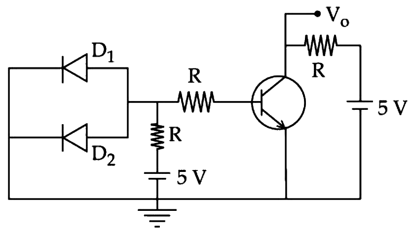
A circuit is arranged as shown in figure. The output voltage V0 is equal to ................... V.
Numerical answer type. Work it out, then open the answer.
Show answer and solution
Answer: 5
Loading the solution…
Report a mistake Q76 NEET 2020 · PHASE 1 Easy Old syllabus ☆
Junction Transistor · Structure & biasing
For transistor action, which of the following statements is correct?
(a) Base, emitter and collector regions should have same size. (b) Both emitter junction as well as the collector junction are forwarded biased. (c) The base region must be very thin and lightly doped. (d) Base, emitter and collector regions should have same doping concentrations. Show answer and solution
Answer: (c)
Loading the solution…
Report a mistake Q77 MHT CET 2020 · 19 OCT · SHIFT 2 Easy ☆
Junction Transistor · Current relations
A transistor having α = 0.8 \alpha = 0.8 α = 0.8
(a) 12 mA (b) 24 mA (c) 0.66 mA (d) 1.5 mA Show answer and solution
Answer: (b)
Loading the solution…
Report a mistake Q78 MHT CET 2020 · 16 OCT · SHIFT 1 Medium ☆
Junction Transistor · CE amplifier gains
In common emitter amplifier, input resistance is 1000 Ω 1000\ \Omega 1000 Ω 5 mV 5\text{ mV} 5 mV β = 60 \beta = 60 β = 60
(a) 3 × 1 0 − 4 A 3 \times 10^{-4}\text{ A} 3 × 1 0 − 4 A (b) 0.5 × 1 0 − 4 A 0.5 \times 10^{-4}\text{ A} 0.5 × 1 0 − 4 A (c) 2 × 1 0 − 5 A 2 \times 10^{-5}\text{ A} 2 × 1 0 − 5 A (d) 1 × 1 0 − 5 A 1 \times 10^{-5}\text{ A} 1 × 1 0 − 5 A Show answer and solution
Answer: (a)
Loading the solution…
Report a mistake Q79 NEET 2020 · PHASE 2 Medium ☆
Junction Transistor · CE amplifier gains
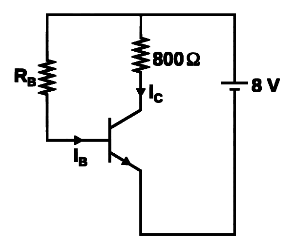
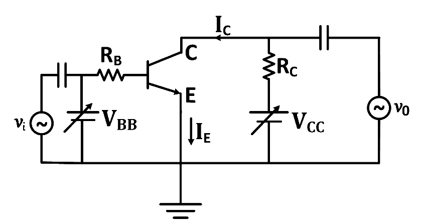
A n-p-n transistor is connected in common emitter configuration (see figure) in which collector voltage drop across load resistance ( 800 Ω ) (800\ \Omega) ( 800 Ω ) 0.8 V 0.8\text{ V} 0.8 V
(a) 0.2 mA 0.2\text{ mA} 0.2 mA (b) 2 mA 2\text{ mA} 2 mA (c) 0.1 mA 0.1\text{ mA} 0.1 mA (d) 1 mA 1\text{ mA} 1 mA Show answer and solution
Answer: (d)
Loading the solution…
Report a mistake Q80 JEE Main 2020 · 6 SEP · SHIFT 2 Medium Old syllabus ☆
Junction Transistor · Characteristics & transistor testing
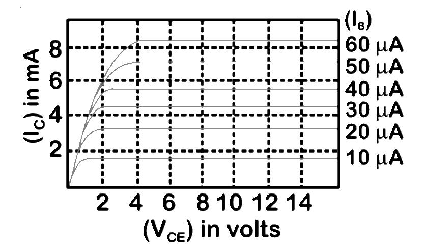
The output characteristics of a transistor is shown in the figure.
When VCE is 10V and IC = 4.0 mA, then value of β \beta β
Numerical answer type. Work it out, then open the answer.
Show answer and solution
Answer: 150
Loading the solution…
Report a mistake Q81 MHT CET 2020 · 16 OCT · SHIFT 2 Medium ☆
Junction Transistor · Switch & oscillator
A A A A A A β A \beta A β A
(a) β A = 0 \beta A = 0 β A = 0 (b) β A = 1 \beta A = 1 β A = 1 (c) β A = ∞ \beta A = \infty β A = ∞ (d) β = 0 \beta = 0 β = 0 Show answer and solution
Answer: (b)
Loading the solution…
Report a mistake Q82 MHT CET 2019 · 3 MAY · SHIFT 1 Easy ☆
Junction Transistor · Structure & biasing
Which of the following regions of a transistors are, respectively, heavily dopped and lightly dopped?
(a) Collector and emitter (b) Base and emitter (c) Emitter and base (d) Emitter and collector Show answer and solution
Answer: (c)
Loading the solution…
Report a mistake Q83 MHT CET 2019 · 2 MAY · SHIFT 2 Easy ☆
Junction Transistor · Current relations
In the study of transistor as an amplifier, the ratio of collector current to emitter current is 0.98 then the ratio of collector current to base current will be
Show answer and solution
Answer: (b)
Loading the solution…
Report a mistake Q84 MHT CET 2019 · 2 MAY · SHIFT 1 Easy ☆
Junction Transistor · Current relations
. For a transistor, the current ratio ' β d c \beta_{dc} β d c
(a) collector current to emitter current. (b) collector current to base current. (c) base current to collector current. (d) emitter current to collector current. Show answer and solution
Answer: (b)
Loading the solution…
Report a mistake Q85 JEE Main 2019 · 10 APR · SHIFT 1 Medium Old syllabus ☆
Junction Transistor · CE amplifier gains
An n-p-n transistor operates as a common emitter amplifier, with a power gain of 60 dB. The input circuit resistance is 100Ω \Omega Ω Ω \Omega Ω β \beta β
(a) 104 (b) 102 (c) 6 × 10² (d) 60 Show answer and solution
Answer: (b)
Loading the solution…
Report a mistake Q86 JEE Main 2019 · 9 APR · SHIFT 1 Medium Old syllabus ☆
Junction Transistor · CE amplifier gains
An NPN transistor is used in common emitter configuration as an amplifier with 1 kΩ \Omega Ω
(a) 0.67 kΩ \Omega Ω (b) 0.33 kΩ \Omega Ω (c) 0.67 kΩ \Omega Ω (d) 0.33 kΩ \Omega Ω Show answer and solution
Answer: (c)
Loading the solution…
Report a mistake Q87 JEE Main 2019 · 12 APR · SHIFT 1 Medium Old syllabus ☆
Junction Transistor · Characteristics & transistor testing
The transfer characteristic curve of a transistor, having input and output resistance 100 Ω \Omega Ω Ω \Omega Ω
(a) 5 × 10⁴, 5 × 10⁵ (b) 5 × 10⁴, 5 × 10⁶ (c) 5 × 10⁴, 2.5 × 10⁶ (d) 2.5 × 10⁴, 2.5 × 10⁶ Show answer and solution
Answer: (c)
Loading the solution…
Report a mistake Q88 JEE Main 2019 · 12 JAN · SHIFT 2 Difficult Old syllabus ☆
Junction Transistor · Current relations
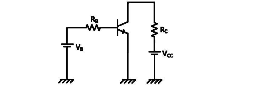
In the figure, given that VBB supply can vary from 0 to 5.0 V, VCC = 5V, β \beta β Ω \Omega Ω Ω \Omega Ω
(a) 20 μ \mu μ (b) 25 μ \mu μ (c) 20 μ \mu μ (d) 25 μ \mu μ Show answer and solution
Answer: (d)
Loading the solution…
Report a mistake Q89 JEE Main 2019 · 8 APR · SHIFT 2 Difficult Old syllabus ☆
Junction Transistor · CE amplifier gains
A common emitter amplifier circuit, built using an npn transistor, is shown in the figure. Its dc current gain is 250, RC = 1kΩ \Omega Ω
(a) 100 μ \mu μ (b) 7 μ \mu μ (c) 10 μ \mu μ (d) 40 μ \mu μ Show answer and solution
Answer: (d)
Loading the solution…
Report a mistake Q90 JEE Main 2018 · 15 APR · SHIFT 1 Easy Old syllabus ☆
Junction Transistor · CE amplifier gains
In a common emitter configuration with suitable bias, it is given that R L R_L R L R B E R_{BE} R BE
β \beta β I B , I C \mathrm{I}_B, \mathrm{I}_C I B , I C I E \mathrm{I}_E I E
(a) β R L R B E , Δ I C Δ I B , β 2 R L R B E \beta\frac{R_L}{R_{BE}}, \frac{\Delta \mathrm{I}_C}{\Delta \mathrm{I}_B}, \beta^2\frac{R_L}{R_{BE}} β R BE R L , Δ I B Δ I C , β 2 R BE R L (b) β R L R B E , Δ I E Δ I B , β 2 R L R B E \beta\frac{R_L}{R_{BE}}, \frac{\Delta \mathrm{I}_E}{\Delta \mathrm{I}_B}, \beta^2\frac{R_L}{R_{BE}} β R BE R L , Δ I B Δ I E , β 2 R BE R L (c) β 2 R L R B E , Δ I C Δ I E , β 2 R L R B E \beta^2\frac{R_L}{R_{BE}}, \frac{\Delta \mathrm{I}_C}{\Delta \mathrm{I}_E}, \beta^2\frac{R_L}{R_{BE}} β 2 R BE R L , Δ I E Δ I C , β 2 R BE R L (d) β 2 R L R B E , Δ I C Δ I B , β R L R B E \beta^2\frac{R_L}{R_{BE}}, \frac{\Delta \mathrm{I}_C}{\Delta \mathrm{I}_B}, \beta\frac{R_L}{R_{BE}} β 2 R BE R L , Δ I B Δ I C , β R BE R L Show answer and solution
Answer: (a)
Loading the solution…
Report a mistake Q91 NEET 2018 Medium Old syllabus ☆
Junction Transistor · Current relations
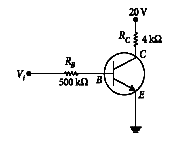
In the circuit shown in the figure, the input voltage Vi is 20 V, VBE = 0 and VCE = 0. The values of IB, IC and β \beta β
(a) IB = 40 μ \mu μ β \beta β (b) IB = 25 μ \mu μ β \beta β (c) IB = 20 μ \mu μ β \beta β (d) IB = 40 μ \mu μ β \beta β Show answer and solution
Answer: (d)
Loading the solution…
Report a mistake Q92 JEE Main 2017 Easy Old syllabus ☆
Junction Transistor · CE amplifier gains
In a common emitter amplifier circuit using an n-p-n transistor, the phase difference between the input and the output voltages will be:
(a) 180° (b) 45° (c) 90° (d) 135° Show answer and solution
Answer: (a)
Loading the solution…
Report a mistake Q93 JEE Main 2017 · 9 APR · SHIFT 1 Medium Old syllabus ☆
Junction Transistor · Current relations
The current gain of a common emitter amplifier is 69. If the emitter current is 7.0 mA, collector current is:
(a) 9.6 mA (b) 6.9 mA (c) 0.69 mA (d) 69 mA Show answer and solution
Answer: (b)
Loading the solution…
Report a mistake Q94 NEET 2017 Medium Old syllabus ☆
Junction Transistor · CE amplifier gains
In a common emitter transistor amplifier the audio sgnal voltage across the collector is 3 V. The resistance of collector is 3 kΩ \Omega Ω Ω \Omega Ω
(a) 15 and 200 (b) 150 and 15000 (c) 20 and 2000 (d) 200 and 1000 Show answer and solution
Answer: (b)
Loading the solution…
Report a mistake Q95 JEE Main 2016 Easy Old syllabus ☆
Junction Transistor · Current relations
For a common emitter configuration, if α \alpha α β \beta β α \alpha α β \beta β
(a) α = β 1 + β \alpha = \frac{\beta}{1+\beta} α = 1 + β β (b) α = β 2 1 + β 2 \alpha = \frac{\beta^2}{1+\beta^2} α = 1 + β 2 β 2 (c) 1 α = 1 β + 1 \frac{1}{\alpha} = \frac{1}{\beta} + 1 α 1 = β 1 + 1 (d) α = β 1 − β 2 \alpha = \frac{\beta}{1-\beta^2} α = 1 − β 2 β Show answer and solution
Answer: (b)
Loading the solution…
Report a mistake Q96 NEET 2016 · PHASE 2 Medium Old syllabus ☆
Junction Transistor · CE amplifier gains
For CE transistor amplifier, the audio signal voltage across the collector resistance of 2 kΩ \Omega Ω Ω \Omega Ω
(a) 10 mV (b) 20 mV (c) 30 mV (d) 15 mV Show answer and solution
Answer: (b)
Loading the solution…
Report a mistake Q97 JEE Main 2016 · 10 APR · SHIFT 1 Medium Old syllabus ☆
Junction Transistor · Characteristics & transistor testing
The ratio (R) of output resistance r0, and the input resistance ri in measurements of input and output characteristics of a transistor is typically in the range:
(a) R ~ 102 − - − (b) R ~ 1 − - − (c) R ~ 0.1 − - − (d) R ~ 0.1 − - − Show answer and solution
Answer: (b)
Loading the solution…
Report a mistake Q98 NEET 2016 · PHASE 1 Difficult Old syllabus ☆
Junction Transistor · CE amplifier gains
A npn transistor is connected in common emitter configuration in a given amplifier. A load resistance of 800 Ω \Omega Ω Ω \Omega Ω
(a) 4, 4 (b) 4, 3.69 (c) 4, 3.84 (d) 3.69, 3.84 Show answer and solution
Answer: (c)
Loading the solution…
Report a mistake Q99 JEE Main 2016 · 10 APR · SHIFT 1 Difficult Old syllabus ☆
Junction Transistor · Characteristics & transistor testing
A realistic graph depicting the variation of the reciprocal of input resistance in an input characteristics measurement in a common emitter transistor configuration is:
Show answer and solution
Answer: (c)
Loading the solution…
Report a mistake Q100 JEE Main 2016 · 9 APR · SHIFT 1 Difficult Old syllabus ☆
Junction Transistor · Characteristics & transistor testing
An unknown transistor needs to be identified as a npn or pnp type. A multimeter, with + ve and − ve terminals, is used to measure resistance between different terminals of transistor. If terminal 2 is the base of the transistor then which of the following is correct for a pnp transistor?
(a) + ve terminal 1, − - − (b) + ve terminal 2, − - − (c) + ve terminal 3, − - − (d) + ve terminal 2, − - − Show answer and solution
Answer: (a)
Loading the solution…
Report a mistake Q101 NEET 2015 · AIPMT Medium Old syllabus ☆
Junction Transistor · CE amplifier gains
The input signal given to a CE amplifier having a voltage gain of 150 is Vi = 2cos(15t + π 3 \frac{\pi}{3} 3 π
(a) 2cos ( 15 t + 5 π 6 ) \left(15t + \frac{5\pi}{6}\right) ( 15 t + 6 5 π ) (b) 300cos ( 15 t + 4 π 3 ) \left(15t + \frac{4\pi}{3}\right) ( 15 t + 3 4 π ) (c) 300cos ( 15 t + π 3 ) \left(15t + \frac{\pi}{3}\right) ( 15 t + 3 π ) (d) 75cos ( 15 t + 2 π 3 ) \left(15t + \frac{2\pi}{3}\right) ( 15 t + 3 2 π ) Show answer and solution
Answer: (b)
Loading the solution…
Report a mistake Q102 JEE Main 2014 · 9 APR · SHIFT 1 Difficult Old syllabus ☆
Junction Transistor · Characteristics & transistor testing
An n-p-n transistor has three leads A, B and C. Connecting B and C by moist fingers, A to the positive lead of an ammeter, and C to the negative lead of the ammeter, one finds large deflection. Then, A, B and C refer respectively to:
(a) Emitter, base and collector (b) Base, emitter and collector (c) Base, collector and emitter (d) Collector, emitter and base. Show answer and solution
Answer: (a)
Loading the solution…
Report a mistake Q103 NEET 2013 Medium Old syllabus ☆
Junction Transistor · Structure & biasing
One way in which the operation of a n-p-n transistor differs from that of a p-n-p
(a) The emitter junction injects minority carriers into the base region of the p-n-p (b) The emitter injects holes into the base of the p-n-p and electrons into the base region of n-p-n (c) The emitter injects holes into the base of n-p-n (d) The emitter junction is reverse biased in n-p-n Show answer and solution
Answer: (b)
Loading the solution…
Report a mistake Q104 NEET 2013 Difficult Old syllabus ☆
Junction Transistor · CE amplifier gains
In a common emitter (CE) amplifier having a voltage gain G, the transistor used has transconductance 0.03 mho and current gain 25. If the above transistor is replaced with another one with transconductance 0.02 mho and current gain 20, the voltage gain will be
(a) 1 3 G \frac{1}{3}G 3 1 G (b) 5 4 G \frac{5}{4}G 4 5 G (c) 2 3 G \frac{2}{3}G 3 2 G (d) 1.5G Show answer and solution
Answer: (c)
Loading the solution…
Report a mistake Q105 NEET 2012 · AIPMT · PRELIMS Easy Old syllabus ☆
Junction Transistor · Switch & oscillator
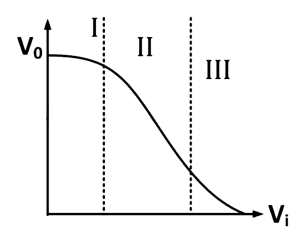
Transfer characteristics [output voltage (V0) vs input voltage (Vi)] for a base biased transistor in CE configuration is as shown in the figure. For using transistor as a switch, it is used
(a) in region III (b) both in region (I) and (III) (c) in region II (d) in region I Show answer and solution
Answer: (b)
Loading the solution…
Report a mistake Q106 NEET 2012 · AIPMT · MAINS Medium Old syllabus ☆
Junction Transistor · CE amplifier gains
The input resistance of a silicon transistor is 100 Ω \Omega Ω μ \mu μ Ω \Omega Ω
(a) 2000 (b) 3000 (c) 4000 (d) 1000 Show answer and solution
Answer: (a)
Loading the solution…
Report a mistake Q107 NEET 2012 · AIPMT · PRELIMS Medium Old syllabus ☆
Junction Transistor · CE amplifier gains
In a CE transistor amplifier, the audio signal voltage across the collector resistance of 2 kΩ \Omega Ω Ω \Omega Ω
(a) 0.1 V (b) 1.0 V (c) 1 mV (d) 10 mV Show answer and solution
Answer: (d)
Loading the solution…
Report a mistake Q108 NEET 2011 · AIPMT · PRELIMS Easy Old syllabus ☆
Junction Transistor · Current relations
A transistor is operated in common emitter configuration at VC = 2 V such that a change in the base current from 100 μ \mu μ μ \mu μ
Show answer and solution
Answer: (a)
Loading the solution…
Report a mistake Q109 NEET 2010 · AIPMT · MAINS Easy Old syllabus ☆
Junction Transistor · Structure & biasing
For transistor action
(1) Base, emitter and collector regions should have similar size and doping concentrations. (2) The base region must be very thin and lightly doped.
(3) The emitter-base junction is forward biased and base-collector junction is reverse biased. (4) Both the emitter-base junction as well as the base-collector junction are forward biased. Which one of the following pairs of statements is correct?
(a) (4) and (1) (b) (1) and (2) (c) (2) and (3) (d) (3) and (4) Show answer and solution
Answer: (c)
Loading the solution…
Report a mistake Q110 NEET 2010 · AIPMT · PRELIMS Easy Old syllabus ☆
Junction Transistor · CE amplifier gains
A common emitter amplifier has a voltage gain of 50, an input impedance of 100 Ω \Omega Ω Ω \Omega Ω
(a) 500 (b) 1000 (c) 1250 (d) 50 Show answer and solution
Answer: (c)
Loading the solution…
Report a mistake Q111 NEET 2009 · AIPMT Easy Old syllabus ☆
Junction Transistor · Current relations
A transistor is operated in common-emitter configuration at VC = 2V such that a change in the base current from 100 μ \mu μ μ \mu μ
Show answer and solution
Answer: (c)
Loading the solution…
Report a mistake Q112 NEET 2008 · AIPMT Medium Old syllabus ☆
Junction Transistor · Switch & oscillator
The voltage gain of an amplifier with 9% negative feedback is 10. The voltage gain without feedback will be
Show answer and solution
Answer: (b)
Loading the solution…
Report a mistake Q113 JEE Main 2008 · AIEEE Difficult Old syllabus ☆
Junction Transistor · Characteristics & transistor testing
A working transistor with its three legs marked P , Q P, Q P , Q R R R P P P Q Q Q R R R P P P Q , Q, Q ,
(a) It is an n p n npn n p n R R R (b) It is an p n p pnp p n p R R R (c) It is an p n p pnp p n p R R R (d) It is an n p n npn n p n R R R Show answer and solution
Answer: (a)
Loading the solution…
Report a mistake Q114 NEET 2007 · AIPMT Easy ☆
Junction Transistor · CE amplifier gains
A common emitter amplifier has a voltage gain of 50, an input impedance of 100 Ω 100\ \Omega 100 Ω 200 Ω 200\ \Omega 200 Ω
(a) 1000 1000 1000 (b) 1250 1250 1250 (c) 100 100 100 (d) 500 500 500 Show answer and solution
Answer: (b)
Loading the solution…
Report a mistake Q115 NEET 2006 · AIPMT Easy Old syllabus ☆
Junction Transistor · Current relations
A transistor is operated in common emitter configuration at constant collector voltage VC = 1.5 V such that a change in the base current from 100 μ \mu μ μ \mu μ β \beta β
Show answer and solution
Answer: (d)
Loading the solution…
Report a mistake Q116 JEE Main 2006 · AIEEE Easy Old syllabus ☆
Junction Transistor · Current relations
In a common base mode of a transistor, the collector current is 5.488 m A 5.488\,mA 5.488 m A 5.60 m A . 5.60\,mA. 5.60 m A . ( β ) (\beta) ( β )
(a) 49 49 49 (b) 50 50 50 (c) 51 51 51 (d) 48 48 48 Show answer and solution
Answer: (a)
Loading the solution…
Report a mistake Q117 JEE Main 2005 · AIEEE Easy Old syllabus ☆
Junction Transistor · CE amplifier gains
In a common base amplifier, the phase difference between the input signal voltage and output voltage is
(a) π \pi π (b) π 4 \frac{\pi}{4} 4 π (c) π 2 \frac{\pi}{2} 2 π (d) 0 0 0 Show answer and solution
Answer: (d)
Loading the solution…
Report a mistake Q118 JEE Main 2004 · AIEEE Easy Old syllabus ☆
Junction Transistor · Structure & biasing
When n p n npn n p n
(a) electrons move from collector to base (b) holes move from emitter to base (c) electrons move from base to collector (d) holes move from base to emitter Show answer and solution
Answer: (c)
Loading the solution…
Report a mistake Q119 JEE Main 2004 · AIEEE Medium Old syllabus ☆
Junction Transistor · CE amplifier gains
For a transistor amplifier in common emitter configuration for load impedance of 1 k Ω ( h f e = 50 1\text{ k}\Omega\ (h_{fe} = 50 1 k Ω ( h f e = 50 h o e = 25 μ A/V ) h_{oe} = 25\ \mu\text{A/V}) h oe = 25 μ A/V )
(a) − 24.8 -24.8 − 24.8 (b) − 15.7 -15.7 − 15.7 (c) − 5.2 -5.2 − 5.2 (d) − 48.78 -48.78 − 48.78 Show answer and solution
Answer: (d)
Loading the solution…
Report a mistake Q120 NEET 2003 · AIPMT Easy Old syllabus ☆
Junction Transistor · Structure & biasing
A n-p-n transistor conducts when
(a) both collector and emitter are positive with respect to the base (b) collector is positive and emitter is negative with respect to the base (c) collector is positive and emitter is at same potential as the base (d) both collector and emitter are negative with respect to the base Show answer and solution
Answer: (b)
Loading the solution…
Report a mistake Q121 JEE Main 2002 · AIEEE Easy Old syllabus ☆
Junction Transistor · Structure & biasing
The part of a transistor which is most heavily doped to produce large number of majority carriers is
(a) emmiter (b) base (c) collector (d) can be any of the above three Show answer and solution
Answer: (a)
Loading the solution…
Report a mistake Q122 NEET 2002 · AIPMT Easy Old syllabus ☆
Junction Transistor · Current relations
For a transistor I C I E \frac{I_C}{I_E} I E I C
Show answer and solution
Answer: (d)
Loading the solution…
Report a mistake Q123 NEET 2001 · AIPMT Easy Old syllabus ☆
Junction Transistor · Current relations
For a common base circuit if I C I E \frac{I_C}{I_E} I E I C
Show answer and solution
Answer: (a)
Loading the solution…
Report a mistake Q124 NEET 2000 · AIPMT Easy Old syllabus ☆
Junction Transistor · Current relations
The correct relation for α , β \alpha, \beta α , β
(a) β = 1 − α α \beta = \frac{1-\alpha}{\alpha} β = α 1 − α (b) β = α 1 − α \beta = \frac{\alpha}{1-\alpha} β = 1 − α α (c) α = β − 1 β \alpha = \frac{\beta-1}{\beta} α = β β − 1 (d) α β = 1 \alpha\beta = 1 α β = 1 Show answer and solution
Answer: (b)
Loading the solution…
Report a mistake Q125 NEET 1998 · AIPMT Medium ☆
Junction Transistor · CE amplifier gains
The transfer ratio β \beta β 50 50 50 1 k Ω 1\text{ k}\Omega 1 k Ω 0.01 V 0.01\text{ V} 0.01 V
(a) 100 μ A 100\ \mu\text{A} 100 μ A (b) 0.01 mA 0.01\text{ mA} 0.01 mA (c) 0.25 mA 0.25\text{ mA} 0.25 mA (d) 500 μ A 500\ \mu\text{A} 500 μ A Show answer and solution
Answer: (d)
Loading the solution…
Report a mistake Q126 NEET 1997 · AIPMT Easy ☆
Junction Transistor · Current relations
The correct relationship between the two current gains α \alpha α β \beta β
(a) α = β 1 + β \alpha = \frac{\beta}{1 + \beta} α = 1 + β β (b) α = 1 + β β \alpha = \frac{1 + \beta}{\beta} α = β 1 + β (c) β = α 1 + α \beta = \frac{\alpha}{1 + \alpha} β = 1 + α α (d) β = α α − 1 \beta = \frac{\alpha}{\alpha - 1} β = α − 1 α Show answer and solution
Answer: (a)
Loading the solution…
Report a mistake Q127 NEET 1996 · AIPMT Easy ☆
Junction Transistor · CE amplifier gains
When npn transistor is used as an amplifier, then
(a) electrons move from collector to base (b) holes move from base to emitter (c) electrons move from base to collector (d) electrons move from emitter to base Show answer and solution
Answer: (c)
Loading the solution…
Report a mistake Q128 NEET 1993 · AIPMT Easy ☆
Junction Transistor · Structure & biasing
The part of the transistor which is heavily doped to produce large number of majority carriers is
(a) emitter (b) base (c) collector (d) any of the above depending upon the nature of transistor Show answer and solution
Answer: (a)
Loading the solution…
Report a mistake Q129 NEET 1991 · AIPMT Easy ☆
Junction Transistor · CE amplifier gains
To use a transistor as an amplifier
(a) the emitter base junction is forward biased and the base collector junction is reversed biased (b) no bias voltage is required (c) both junction are forward biased (d) both junction are reverse biased Show answer and solution
Answer: (a)
Loading the solution…
Report a mistake Q130 NEET 1990 · AIPMT Easy ☆
Junction Transistor · CE amplifier gains
In a common base amplifier the phase difference between the input signal voltage and the output voltage is
(a) 0 0 0 (b) π 4 \frac{\pi}{4} 4 π (c) π 2 \frac{\pi}{2} 2 π (d) π \pi π Show answer and solution
Answer: (a)
Loading the solution…
Report a mistake Q131 NEET 1989 · AIPMT Easy Old syllabus ☆
Junction Transistor · Switch & oscillator
Radiowaves of constant amplitude can be generated with
(a) FET (b) filter (c) rectifier (d) oscillator Show answer and solution
Answer: (d)
Loading the solution…
Report a mistake
No questions match these filters.